Battery Energy Storage (ESS) solutions are not only used in industrial and power generation applications, but also in the residential part of the family, which has become the key to the current application and market development. Residential ESS solutions require less power, but still have the same conversion efficiency and safety requirements as industrial applications. In this article, we will introduce you to the market trend of residential ESS solutions, and introduce the functional characteristics of SiC-related solutions.
Residential ESS for Storing and Managing Energy
Residential ESS is an energy storage solution used in homes to store and manage electrical energy to improve energy efficiency, reduce energy costs, and increase the stability of the energy supply. Residential ESS applications typically include solar power generation systems (photovoltaic (PV) systems), where solar PV panels are typically mounted on the roof or other appropriate location to convert sunlight into direct current (DC) electrical energy.
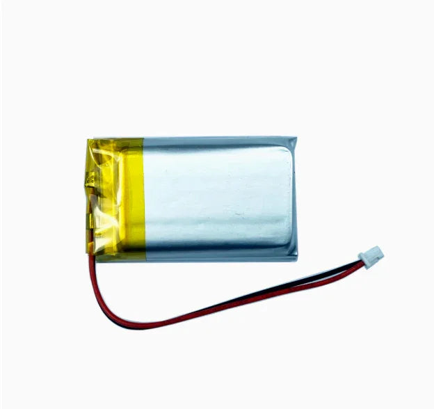
An ESS also requires a charge controller that is responsible for monitoring the output of the solar power system and controlling the flow of electricity to the energy storage system, which ensures that the solar-generated electricity is stored in a battery. Batteries are the core component of the ESS and are used to store the solar-generated electricity during the day to supply energy at night or on cloudy days. Common battery technologies available today include lithium-ion (Li-ion) and lead-acid batteries.
The ESS also requires an inverter to convert the DC power stored in the batteries to AC power to supply appliances and lighting in the home, and an energy management system (EMS) to monitor the home's energy usage, weather forecasts, and electricity prices to optimize energy use and storage. It can automatically control the charging and discharging process to ensure optimal energy efficiency.
The residential ESS can also be connected to the grid, enabling households to purchase electricity when needed or sell excess energy to the grid when there is sufficient energy - this ability to flow energy in both directions is known as 'two-way metering'. Through the monitoring system, householders can monitor the operational status of the energy system, energy generation and consumption in real time, and make operational adjustments through the remote control system, such as changing the operating mode of the energy storage system or setting the charging and discharging times.
The architecture of a residential ESS can be adapted to specific needs and technologies to ensure optimal performance and efficiency. Such systems help to achieve energy self-sufficiency, save energy and reduce emissions, and provide back-up power in the event of a grid outage.
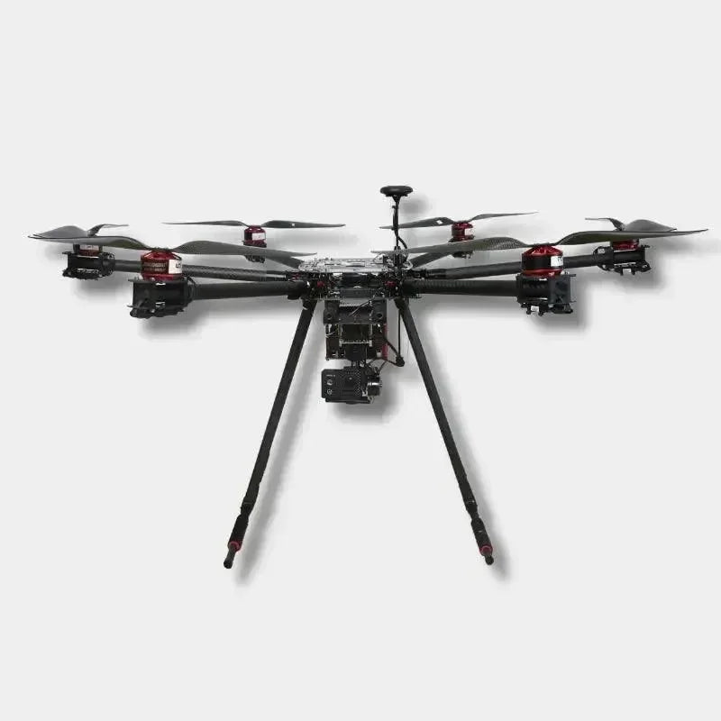
Residential ESS applications differ from industrial applications in terms of requirements, with the main differences being that residential ESSs require lower power, typically less than 10kW, must support bi-directional power conversion, mostly use high efficiency AC/DC topologies with high EMC characteristics, as well as high efficiency DC/DC topologies with high safety specifications, and must support a wide range of bus voltages from 360V - 550V The batteries are usually placed on the DC side, requiring system efficiency of more than 90% and reliable system stability, the pursuit of high power density, to achieve the goal of small size and light weight, and the need to reduce the system cost, and the requirements of safety, EMC, noise and other characteristics of the higher requirements.
SiC Outperforms Silicon Devices
In order to meet the above requirements, Silicon Carbide (SiC) is often required for power conversion, due to some significant advantages of SiC devices, which can improve system efficiency at high currents and high temperatures, and the high electric field toughness of SiC materials allows SiC devices to operate at higher voltages, with higher withstand voltages compared to silicon devices, which makes SiC devices particularly useful in power conversion applications.
This makes SiC devices particularly useful in power conversion applications.
In addition, SiC devices have a higher electron migration rate, which makes them superior in high frequency applications. For applications such as high-frequency converters and power amplifiers, SiC devices offer improved performance. the thermal conductivity of SiC is three times that of silicon and allows for smaller size and weight to increase power density, optimize system cost, reduce cost per unit of volume, convert energy in both directions, and be safe and reliable, achieving a 50% reduction in size and lower cost per watt, meaning that Smaller and lighter devices at the same power level.
SiC materials are chemically stable and less susceptible to corrosive substances. This makes SiC devices more suitable for applications in some extreme environments.SiC devices have high carrier movement speeds, which gives them faster switching speeds. This is beneficial for reducing switching losses, increasing conversion efficiency, and improving device dynamics.
The use of SiC energy storage solutions can have a smaller product size and weight, can achieve higher switching frequency, and due to the use of smaller magnetic devices, can use smaller transformers / inductors, its loss is smaller, better heat dissipation, the same power can be mounted in a smaller enclosure, and compared with silicon IGBTs, SiC power density (W / Kg) doubled, with a high power density, and can use the Simple bi-directional converter topology with less loop control and higher efficiency.
SiC devices have lower on-resistance per unit volume, low conduction losses, no current drag during turn-off, low switching losses, and very low body diode recovery losses, and can reduce the bill of materials content (BOM), system ruggedness and higher reliability.
DC-DC high-voltage side of the design, for example, in the bus voltage 500V can be used 1200V SiC and IGBT, drive voltage 15V / -2.5V, switching frequency of 30kHz, the other side of the circuit can be used in 650V SiC and IGBT, drive voltage 15V / -2.5V, switching frequency of 76kHz. high-voltage side of the circuit when the SiC device efficiency Higher efficiency when SiC devices are used in the high voltage side circuit, SiC power tubes are driven by 15V and are compatible with IGBT power tube solutions.

Challenges and Solutions for Bidirectional DC/DC Converters
There are many challenges in designing a bi-directional DC/DC power converter for ESS, such as solving the problem of low-side MOS Vds stress in steady state operation and no-load condition in discharge mode, and the solution is to increase the inductance in the primary of the transformer to 200µH, which reduces the voltage stress by 25%, and improves the efficiency by 6%~7%.
In addition, to solve the problem of Vds voltage stress in discharge mode and startup, the solution is to use PWM+PFM hybrid control at the input port, which will reduce the voltage stress by 27%, and the Vmax is 124V at 80V. Similarly, in discharge mode, the resonant capacitor needs to face the abnormally high temperature (96℃@2100W), and the capacitor can be changed to mkp21224/400VDC, which will reduce the voltage stress by 25% and improve the efficiency by 6%~7%. /400VDC, the resonant capacitor temperature can be reduced to 65℃@3000W.
On the other hand, in the discharge mode, the operating frequency will suddenly change to 180 kHz, and the gain curve is not stable. In this case, the gain curve can be kept stable by tuning the SRMOS fixed on-time frequency point to below 180 kHz.

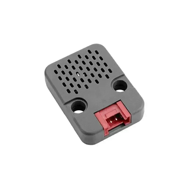
SiC MOSFET Products Meet DC-DC Design Needs
Taking the 6600V 48V bidirectional high-frequency isolated DC-DC reference design as an example, its charging part can support a DC bus charging range of 380-480 VDC, DC bus charging current ≦16A, output voltage of 40-60 VDC, output current ≦140A, output power of up to 6.6 kW, charging efficiency of up to 95% at 420V, charging current ripple factor is 1%. In the discharge section, the battery side voltage range is 40-60 VDC, the battery side current≦140A, the DC bus voltage range is 380-480 VDC, the output power is up to 6.6 kW, the discharge efficiency is up to 94% at 54V, and the bus voltage ripple coefficient is 1%.
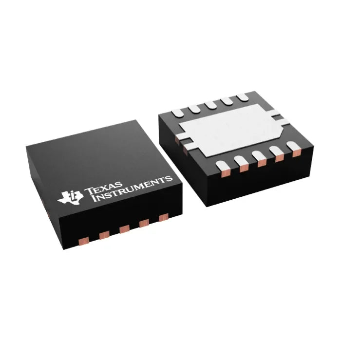
This reference design operates from 43V-57V on the low voltage side without the Buck_Boost regulator, and from 49V-57V at full power, with a maximum stabilized output current of 142A and a maximum short-time output current of 150A (Vin = 420V, resistive load). With the Buck_Boost regulator, the low voltage side operates from 43V-57V, the full power operating range is 49V-60V, the maximum stabilized output current is 145A, and the maximum short-time output current is 150A (Vin = 420V, resistive load). This reference design utilizes eight of Rohm's SCT3030AR TO-247 packaged SiC MOSFETs, as well as the BM61S41RFV-C gate driver with RJ1P12BBDTLL power MOSFETs.
Rohm's SCT3030AR is a SiC MOSFET supporting 650V Nch in a 4-pin package, and is a trench gate SiC MOSFET ideally suited for server power supplies, solar inverters, and electric vehicle charging stations that require high efficiencies, etc. It is available in a 4-pin package that separates the power supply source pin from the driver source pin, which maximizes high-speed switching performance. In particular, it significantly improves conduction loss, reducing conduction loss and turn-off loss by a combined total of approximately 35% compared to the previous 3-pin package (TO-247N).
Rohm's SCT3030AR features low on-resistance, fast switching speed, fast reverse recovery, easy paralleling, and simple driving, and is available in a lead-free plated package that is RoHS compliant for a wide range of applications such as solar inverters, DC/DC converters, switching power supplies, induction heating, and motor drives.
BM61S41RFV-C is a gate driver with isolation voltage of 3750 Vrms, maximum gate drive voltage of 24V, maximum I/O delay time of 65 ns, minimum input pulse width of 60 ns, output current of 4A, under voltage lockout (UVLO) function and active Miller clamp function, compliant with AEC-Q100 standard, and adopts SSOP-B10W package. The RJ1P12BBD is a Nch 100V 120A power MOSFET with low on-resistance, high power in a small die package, lead-free plating, RoHS compliant, halogen-free and UIS tested.
Conclusion
As green energy becomes more and more important to the international community, it is also driving the rapid development of residential ESS applications, which involves a considerable number of electronic components and solutions, and also represents a huge market opportunity.